
Applied Materials expands Singapore operations to support growing global demand for AI chips
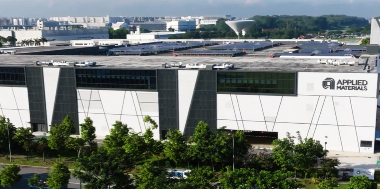
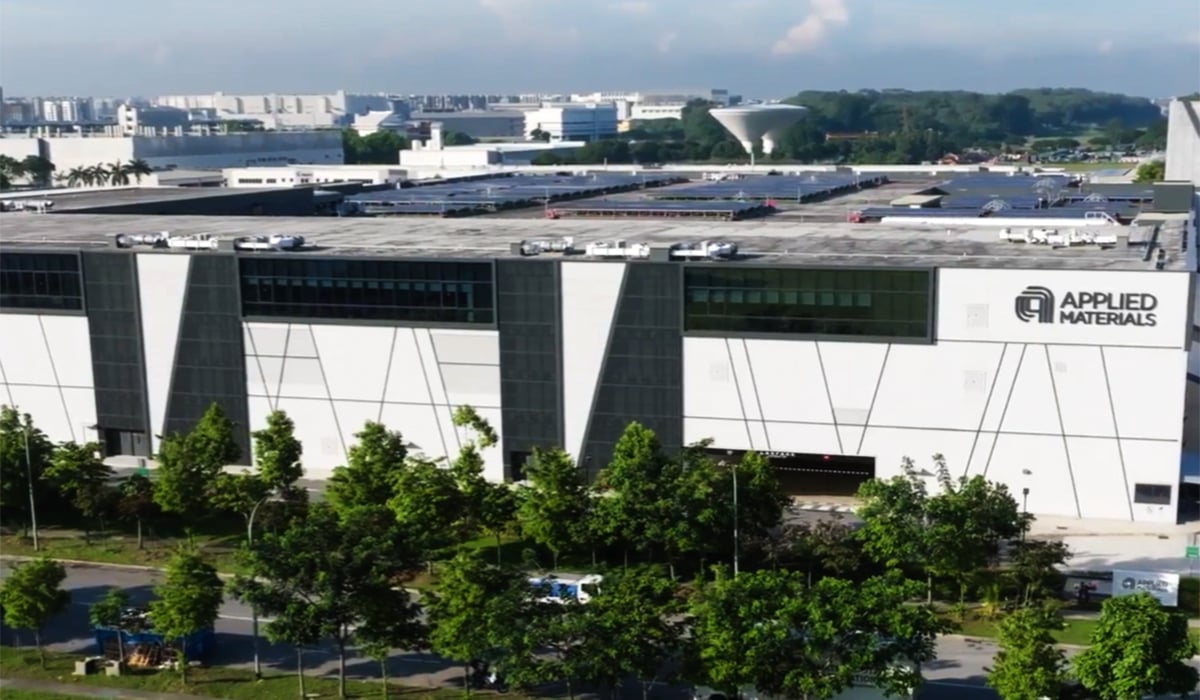
Semiconductor equipment manufacturer Applied Materials has officially expanded its operations in Singapore with the opening of its new S$600 million Tampines Campus.
Announced on Tuesday (10 June), the facility is already operating at volume production and will support chipmakers worldwide as they ramp up manufacturing to meet growing demand driven by artificial intelligence (AI).
The new campus more than doubles the company’s advanced cleanroom capacity in Singapore, strengthening its global manufacturing network alongside facilities in the United States, Europe, Israel, and Taiwan.
Expansion expected to create around 1,000 jobs
As part of its Singapore 2030 growth plans, Applied Materials expects to create approximately 1,000 new jobs in Singapore over the next few years.
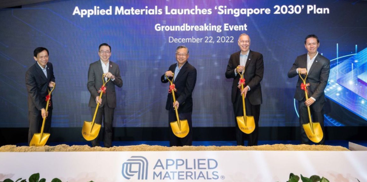
Source: Gan Kim Yong on LinkedIn
The roles will support manufacturing, research and development (R&D), and the commercialisation of new technologies.
According to KC Ong, Group Vice President of Worldwide Manufacturing at Applied Materials, the company has operated in Singapore for 35 years and views the country as a key hub in its global operations.
“Our new AI-enabled, automation-ready facility represents the next era of advanced manufacturing optimized for speed, precision, and quality,” Mr Ong said.
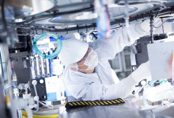
New facility equipped with AI and automation technologies
The Tampines Campus incorporates a range of advanced technologies aimed at improving manufacturing efficiency.
These include Autonomous Mobile Robots (AMRs), autonomous assembly and testing systems, as well as AI-assisted quality inspection processes.
Source: Applied Materials
The company also uses augmented reality (AR) and virtual reality (VR) tools to train technicians and support maintenance work.
Applied Materials said the integration of manufacturing and R&D operations at the site will help accelerate the development and rollout of new semiconductor technologies.
Campus designed with sustainability in mind
Beyond manufacturing capabilities, the new campus has also been designed with sustainability as a key focus.
Applied Materials said the facility is targeting Building and Construction Authority (BCA) Green Mark Platinum certification, the highest tier under Singapore’s green building rating scheme.
Features include an onsite solar panel system, energy-efficient LED lighting, low-carbon concrete construction, and a closed-loop water reclamation system designed to achieve zero water waste.
Source: Applied Materials
A Smart Building Management System will also monitor energy and water consumption in real time.
Expansion strengthens Singapore’s semiconductor ecosystem
Applied Materials President and CEO Gary Dickerson said AI is creating unprecedented demand for advanced semiconductors across industries.
He added that the company’s expanded Singapore operations will help it deliver semiconductor manufacturing equipment more efficiently, allowing chipmakers to bring next-generation technologies to market faster.
Singapore Economic Development Board (EDB) chairman Png Cheong Boon noted that the new campus will help in accelerating product development and increasing Singapore’s manufacturing capabilities.
“We welcome this expansion that will strengthen our vibrant semiconductor ecosystem, creating quality jobs and opportunities for Singaporeans.”
Also Read: 50% of S’pore finance professionals fear AI could affect their jobs, 59% don’t trust AI in hiring
50% of S’pore finance professionals fear AI could affect their jobs, 59% don’t trust AI in hiring
Have news you must share? Get in touch with us via email at news@mustsharenews.com.
Featured image adapted from Applied Materials.